
You would possibly discover previous digital merchandise that aren’t supported anymore. In case you reverse engineer circuit board components from these, you may repair and enhance them. Many individuals do that to restore previous devices or make them last more.
Some need to keep away from deliberate obsolescence. Typically, it’s good to reverse engineer circuit board layouts in the event you can not discover schematics or restore guides.
Folks reverse engineer circuit board elements for various causes:
- To switch previous boards in discontinued digital merchandise
- To rebuild schematics from {hardware} in discontinued digital merchandise
- To make working replacements for discontinued digital merchandise
It’s also possible to use IC decryption to unlock chips. This helps you deal with previous methods. In case you study PCB reverse engineering, you may hold previous digital merchandise working for a few years.
Key Takeaways
- PCB reverse engineering allows you to repair previous electronics. You can also make new schematics and hold gadgets working longer.
- Use a transparent step-by-step course of for reverse engineering. Checklist all components, take photos of the PCB, and replica the format to be correct.
- Use the best instruments for good PCB evaluation. Digital multimeters and X-ray inspection provide help to get vital knowledge.
- Know the authorized and moral guidelines for PCB reverse engineering. At all times ask for permission and respect authentic designs to keep away from hassle.
- IC unlock strategies can get helpful knowledge from chips. Use direct readout or glitching assaults to get data safely.
PCB Reverse Engineering Fundamentals
What’s PCB Reverse Engineering
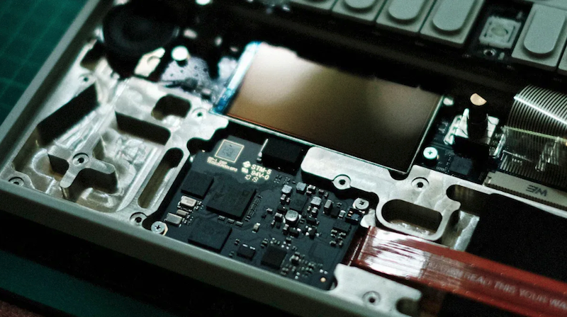
PCB reverse engineering helps you determine how a circuit board works. You begin with a completed pcb and attempt to make a schematic. This allows you to see how components join and the way alerts transfer.
Printed circuit board reverse engineering means you are taking aside a pcb to study its design. You can also make new paperwork or enhance the board.
PCB reverse engineering will not be the identical as PCB copy and IC unlock. PCB reverse engineering appears on the board and its connections. You test how components hyperlink and the way alerts journey. IC decryption is about unlocking the code inside a chip. You need to copy or examine this system knowledge within the chip.
Whenever you reverse engineer a pcb, you usually rebuild the schematic. This exhibits how every half works with others. You employ the schematic for repairs, upgrades, or making new boards. It additionally helps you discover issues if one thing breaks.
Tip: Set clear targets earlier than you begin. Resolve if you wish to repair, improve, or simply study in regards to the pcb. This can provide help to acquire the best knowledge.
Key Steps to Reverse Engineer Circuit Board
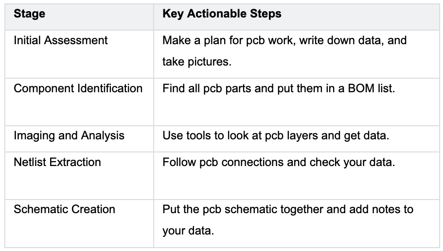
There’s a easy path for pcb reverse engineering. Every step helps you collect knowledge and construct a schematic. Listed here are the primary steps:
- Cataloging Parts: Write down each half on the pcb. Make a Invoice of Supplies (BOM) listing. This helps you discover components and construct the schematic.
- Eradicating Parts (If Wanted): Take off components rigorously if it’s good to see traces or take a look at them. Preserve observe of the place every half goes.
- Photographing and Scanning the PCB: Take clear photos of either side of the pcb. These images provide help to map out traces and connections.
- Picture Correction and Hint Mapping: Edit your images to make traces simpler to see. This helps you draw the schematic.
- Figuring out Pads, Traces, and Vias: Mark each pad, hint, and through. This step helps you discover components and see how alerts transfer.
- Aligning and Layering Photographs for Double-Sided Boards: Line up photographs from either side. This helps you see how traces join by means of the board.
- Recreating the PCB Structure in Design Software program: Use software program to attract the board. You can also make a brand new schematic and recordsdata for a brand new pcb.
- Making a Invoice of Supplies (BOM): Checklist all components and their particulars. This helps with repairs and future evaluation.
- Testing and Troubleshooting: Test your work. Check the board and search for issues. Use failure evaluation if one thing doesn’t work.
For multi-layer boards, you repeat some steps. You scan or picture every layer. This provides you all the info you want for a full schematic and evaluation.
Word: In case you skip steps or miss knowledge, you’ll have hassle discovering alerts or components later.
Instruments and Imaging Strategies
You want the best instruments for pcb reverse engineering. Some instruments provide help to discover components, others provide help to acquire knowledge or construct the schematic. Listed here are some widespread instruments:
- Digital Multimeter (DMM): Measures voltage, present, and resistance. You employ it for fast checks and alerts.
- SMD LCR Meter: Measures small components like capacitors and resistors. It helps you discover components.
- Energy Provide: Helps you to take a look at the pcb and see the way it handles alerts.
- Common Machine Programmer: Packages chips and helps with deeper knowledge evaluation.
- Multi-Protocol Adapter: Talks to totally different chips and helps with knowledge assortment.
For imaging, you’ve gotten many decisions. Some work higher for single-layer boards, others are greatest for multi-layer boards. Here’s a desk of widespread imaging strategies:
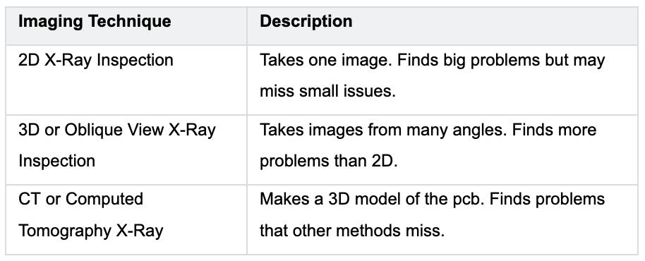
X-ray methods allow you to see inside a pcb with out taking it aside. These methods discover issues like unhealthy solder joints or misaligned components. They will see tiny gaps as small as 10 micrometers.
Fashionable pcb reverse engineering makes use of new strategies. Automated Optical Inspection (AOI) makes use of cameras and AI to seek out components and traces. 3D X-ray CT makes detailed fashions of the within of a pcb. Electromagnetic Discipline Evaluation allows you to examine alerts and knowledge with out opening the board. These instruments provide help to acquire higher knowledge and make a extra correct schematic.
Alert: At all times test your schematic and knowledge earlier than making a brand new pcb. Errors find components or alerts could cause issues later.
You must know the most effective methods for single-layer and multi-layer boards. For single-layer boards, you may usually see all traces and pads. For multi-layer boards, you want imaging or cautious delamination.
At all times hold your knowledge organized. Use clear labels for each half and sign. This helps with schematic work and discovering issues.
In case you observe these steps and use the best instruments, you are able to do pcb reverse engineering properly. You’re going to get a transparent schematic, good knowledge, and a working board.
PCB Copy and Clone
What’s PCB Copy vs. PCB Clone
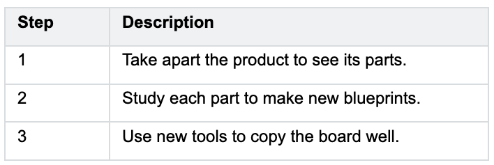
Chances are you’ll hear folks use the phrases pcb copy and pcb clone. These phrases sound related, however they’ve totally different meanings in pcb reverse engineering. Whenever you copy a pcb, you make a precise reproduction of the unique board.
You employ pcb reverse engineering to match the format, components, and connections. Cloning a pcb goes additional. You possibly can copy the board, however you might also change or enhance the design. Cloning allows you to add new options or repair previous issues. Each strategies provide help to save money and time by utilizing present knowledge as an alternative of ranging from scratch.
Step-by-Step Course of for PCB Copying
You possibly can observe a transparent course of to repeat a pcb. Every step helps you acquire knowledge and rebuild the board:
- Preparation: Clear the pcb and take away any coatings. Take out elements so you may see all traces and pads. This step helps you get good knowledge for the subsequent steps.
- Schematic Technology: Hint all connections and establish every half. Use pcb reverse engineering to create a digital schematic. This schematic exhibits how alerts transfer and the way components join.
- PCB Structure Reconstruction: Place every half in the best spot. Draw all traces and test your work. Use design software program to ensure your knowledge matches the unique pcb.
- Invoice of Supplies (BOM) Creation: Checklist each half and its particulars. This knowledge helps you discover and purchase the best elements in your new pcb.
Key Concerns and High quality Management
You might want to test your work at each step. Good high quality management retains your pcb working properly. Use this desk to information your checks:
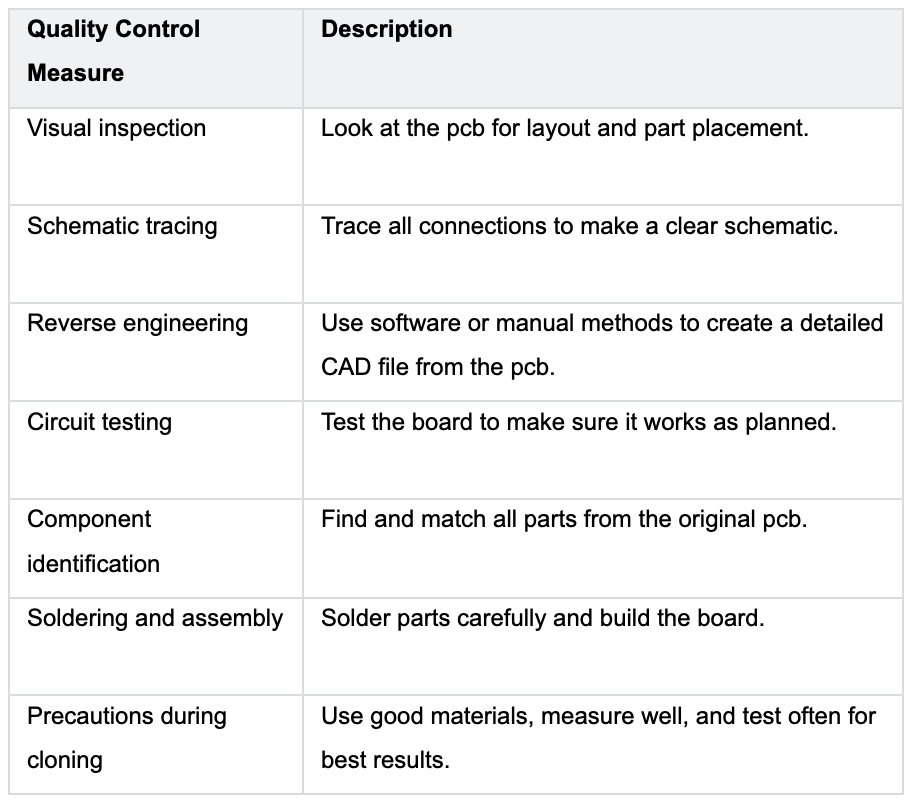
Tip: At all times double-check your knowledge and connections. Use high-quality instruments and supplies. Check your cloned pcb with the unique gadget to ensure it really works.
Typical Functions and Limitations
You employ pcb reverse engineering to repeat or clone boards for a lot of causes. You possibly can hold previous machines working once you can not purchase new components.
You should use pcb reverse engineering to rebuild misplaced knowledge or restore a design when the maker stops making the product. Many individuals use pcb reverse engineering to repair industrial management methods or different vital gear.
Chances are you’ll face some limits. Complicated boards with many layers or hidden components could make pcb reverse engineering exhausting. In case you use poor components, your pcb could not work properly.
It’s essential to take a look at your knowledge and board to keep away from issues. Copying or cloning a pcb with out permission can break the legislation, so all the time test earlier than you begin.
IC Unlock and Decryption
Superior IC Unlock
Typically, you need to discover out what’s inside an ic. This helps you find out how the ic works and shops knowledge. You employ IC unlock to repair, copy, or make previous electronics higher. Many individuals use IC decryption with pcb reverse engineering and iwm reverse engineering to maintain gadgets working.
There are alternative ways to check an ic. These strategies provide help to get the format and discover hidden knowledge. The desk under exhibits some good strategies:
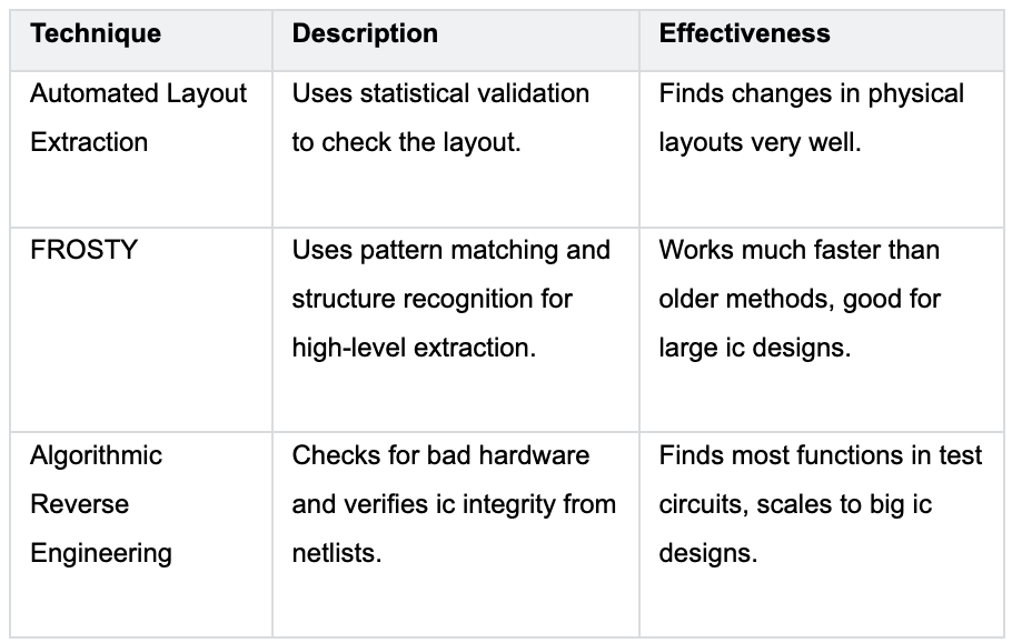
These strategies provide help to see the ic clearly. Automated format extraction helps you see errors within the chip. FROSTY allows you to work quick, even with large ic layouts.
Algorithmic reverse engineering helps you discover hidden issues or further circuits. In case you use these with pcb reverse engineering and iwm reverse engineering, you may perceive the entire gadget.
Tip: Preserve your knowledge neat and arranged. Good notes provide help to match ic layouts with pcb traces and iwm reverse engineering outcomes.
MCU Unlocking Strategies
Microcontroller models (MCUs) management how a pcb works. Chances are you’ll have to unlock an mcu to get the info inside. This step is vital for iwm reverse engineering and pcb reverse engineering. There are a number of methods to unlock an mcu:
- Direct Readout: You employ a programmer to learn the ic instantly. This works if the ic doesn’t have sturdy safety.
- Glitching Assaults: You ship particular alerts to the ic to make it skip safety checks. This technique may also help you get the info if the ic has fundamental safety.
- Decapsulation: You take away the highest of the ic and use a microscope to see the info saved inside. This technique is gradual however works for some chips.
- Aspect-Channel Assaults: You measure issues like energy use or temperature modifications whereas the ic runs. These modifications can present you the info contained in the ic.
- Firmware Extraction: You employ particular instruments to tug the firmware from the ic. This technique helps you get the code and knowledge for iwm reverse engineering.
Choose the strategy that matches your ic and your objective. Some strategies work higher for easy chips. Others are greatest for complicated or protected ics. At all times test your outcomes with pcb reverse engineering and iwm reverse engineering to ensure your knowledge is correct.
Word: Some unlocking strategies can break the ic. Observe on spare chips earlier than engaged on uncommon or vital gadgets.
Challenges and Options
You’ll face many issues once you attempt ic unlock. Some ics use weak encryption. Attackers can discover these weak spots and get the info. Aspect-channel assaults can even assist attackers.
They look ahead to small modifications in energy or temperature to seek out secrets and techniques contained in the ic. Manufacturing errors could make issues worse. If corporations don’t take a look at safety properly or observe requirements, attackers can break into the ic extra simply.
You should use some options to make ic decryption tougher for attackers:
- Use sturdy cryptographic strategies and {hardware} safety modules. These instruments shield the info contained in the ic.
- Add code obfuscation. This makes it tougher for attackers to make use of iwm reverse engineering or pcb reverse engineering to learn how the ic works.
- Rotate keys usually and use safe enclaves. These steps hold delicate knowledge secure, even when somebody will get into the ic.
At all times test your safety. Common testing helps you discover weak spots earlier than attackers do. Whenever you use pcb reverse engineering, PCB copy, and ic decryption collectively, you may hold your gadgets secure and dealing.
Alert: By no means skip safety checks. Good safety retains your knowledge and gadgets secure from hurt.
Motivations for Discontinued Digital Merchandise
Restore and Restoration
You would possibly need to repair or convey again previous electronics that aren’t made anymore. Whenever you use pcb reverse engineering, you may make these merchandise work once more. First, you are taking aside the pcb and have a look at every half.
You write down how the components are arrange and related. This helps you see how the pcb works. After that, you may draw a brand new schematic and construct new boards if it’s good to. The desk under exhibits how you utilize pcb reverse engineering for fixing and restoring:
It’s essential to acquire knowledge at each step. This knowledge helps you discover what’s damaged and swap out unhealthy components. You additionally use the info to check the pcb and test if it really works like earlier than.
Replication and Enhancement
Typically, you need to make a duplicate of a pcb or make it higher. You employ pcb reverse engineering to get knowledge from the previous board. This knowledge allows you to construct a brand new pcb that is rather like the previous one. It’s also possible to use the info so as to add new issues or repair issues.
For instance, you would possibly put in higher connectors or change the format to work quicker. You might want to test your knowledge many occasions so you don’t make errors. Whenever you end, you’ve gotten a pcb that works properly and is likely to be even higher than earlier than.
Tip: At all times hold your knowledge neat and simple to seek out. Good notes provide help to make good copies and simple upgrades.
Innovation and Analysis
You should use pcb reverse engineering to study new issues and make higher merchandise. Whenever you have a look at previous pcb designs, you get knowledge that exhibits how folks solved issues earlier than.
This knowledge helps you study previous methods and discover methods to make them higher. You should use the info for analysis or to construct new issues. Listed here are some methods pcb reverse engineering helps with new concepts and analysis:
- You learn to repair and improve previous methods.
- You have a look at different designs to get new concepts and make your individual pcb higher.
- You save time and cash by utilizing knowledge from previous merchandise.
- You’re employed quicker by utilizing knowledge and layouts that already work.
You assist the electronics world develop once you use pcb reverse engineering. You flip previous knowledge into new solutions.
Authorized & Moral Points
Authorized Restrictions
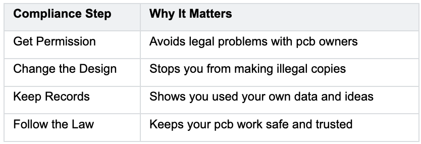
It’s essential to know the legal guidelines earlier than you begin pcb reverse engineering. Many nations shield designs with patents and commerce secrets and techniques. In case you copy a pcb with out permission, you may break the legislation. Some legal guidelines, just like the DMCA, allow you to reverse engineer for studying or fixing, however you can’t break safety features.
You must all the time test if the pcb design is public or you probably have written permission. In case you use somebody’s knowledge with out asking, you may face authorized hassle. It’s essential to additionally keep away from making pretend merchandise that seem like the actual factor.
Moral Concerns
You must take into consideration what is correct and honest once you work with pcb reverse engineering. In case you use knowledge from a pcb, you should respect the work of others. Don’t use knowledge to make copies that trick folks.
You should use pcb reverse engineering to repair, study, or enhance, however to not steal concepts. Sharing knowledge for studying helps everybody, however promoting pretend boards hurts belief. You must all the time inform the place your knowledge comes from and provides credit score once you use somebody’s work.
Tip: Ask your self in case your work helps others or simply copies another person’s concepts. Good ethics construct belief within the tech world.
Compliance Ideas
You possibly can observe these steps to remain secure and authorized once you use pcb reverse engineering and knowledge:
- Get authorized permission or test that the pcb is within the public area.
- Use pcb reverse engineering to study or enhance, to not make actual copies.
- Preserve good data of your scans, exams, and knowledge decisions.
- Know the legal guidelines in your nation, just like the DMCA, and don’t break safety on objective.
In case you observe these steps, you should use pcb reverse engineering and knowledge in a wise and secure method. You shield your self and respect the work of others.
You are able to do pcb reverse engineering and IC unlock properly in the event you observe easy steps. The desk under exhibits what to do with pcb and knowledge at every step:
You must use good instruments, hold your knowledge neat, and act truthfully. Some useful books are The Artwork of PCB Reverse Engineering, PCB-RE: Instruments & Strategies, and PCB-RE: Actual-World Examples.
Specialists say you need to attempt new issues but in addition observe the legislation. You possibly can be a part of teams, share pcb knowledge, and study from different folks. At all times use pcb reverse engineering in a great way and assist others by sharing your knowledge.
FAQ
What’s PCB reverse engineering?
You employ PCB reverse engineering to check a circuit board. You acquire knowledge about components and connections. This helps you perceive how the board works and allows you to repair or copy it.
How do you acquire knowledge from a discontinued digital product?
You begin by taking clear images. You write down every half and hint connections. You employ instruments to scan layers. You arrange all knowledge so you may construct a brand new schematic.
Why is knowledge vital in IC unlock?
You want knowledge to unlock and examine chips. Knowledge exhibits how the chip shops data. You employ knowledge to seek out weak spots and perceive the chip’s capabilities.
Can you utilize knowledge to enhance previous gadgets?
You should use knowledge from previous boards to make upgrades. Knowledge helps you see issues and add new options. You construct higher gadgets by utilizing knowledge from previous designs.
What instruments provide help to analyze knowledge in PCB reverse engineering?
You employ a multimeter, scanner, and design software program. These instruments provide help to acquire and test knowledge. You arrange knowledge to make schematics and take a look at boards.


